Evident offers a wide range of optical components that can be combined with various microscope-based imaging devices for fields such as life science research, medical care, and manufacturing.
To help equipment designers optimize their devices, we are always working to develop objective lenses with the latest technological advances. As part of this effort, we recently looked at how objective lens technology can improve throughput in industrial inspections.
Throughput (the number of inspections that can be processed within a certain amount of time) is a common challenge for designers developing devices for semiconductor, flat panel display (FPD), and organic light-emitting diode (OLED) inspections. This post covers a newly developed objective series that can improve inspection throughput.
Overcoming Limitations in Throughput for Semiconductor Wafer Inspections
Typically, an objective with a shorter working distance (WD) must be used reach the desired resolution for a wafer inspection. Retracting the nosepiece during wafer exchange is necessary when using an objective with a short working distance, as the shorter distance between the objective and wafer could lead to a collision. However, the time it takes to move the microscope nosepiece up and down for the wafer exchange adds to the overall inspection time and limits throughput.
 |  |
Comparing objectives with shorter and longer working distances (left: 1 mm WD, right: 3 mm WD) but the same magnification and numerical aperture. The objective with the longer working distance (right) provides more room between the objective and the sample, minimizing the risk of a collision.
Our customers wanted their devices to acquire high-resolution images and enable the high-speed transport of semiconductor wafers, FPD boards, and other samples, all without retracting or switching the objective lens.
Meeting these demands requires an objective with both a long working distance and high resolution, which presented us with a challenge. In general, an objective’s working distance decreases as its magnification and numerical aperture (resolution) increases, so our existing objective lineup was divided into high-resolution lenses and long working distance lenses.
We decided to create a new objective series to give customers what they wanted: high resolution and a long working distance simultaneously. This innovation resulted in our new MXPLFLN objective series.
Introducing the MXPLFLN Objective Series for High-Throughput Inspections
Our new MXPLFLN series takes high-resolution images with a larger view field of view and high flatness (image uniformity from the center to the edge). These features are ideal for image stitching. A wider field of view means you need to stitch together fewer images to cover the entire inspection area, while high-resolution, flat images stitch together seamlessly. In terms of flatness, this objective series is designed to achieve peak performance in combination with our newly designed U-SWATLU tube lens. We recommend combining them to achieve further improvement in throughput.

U-SWATLU tube lens
Our MXPLFLN series features objectives with 20X and 50X magnifications. Both magnifications are available in brightfield only and brightfield/darkfield options. Let’s take a look at their features.
MXPLFLN20X and MXPLFLN20XBD 20X Objective Lenses
With our new manufacturing technology, the brightfield version of the 20X objective (MXFPLFLN20X) offers an increased NA from 0.45 to 0.6 with a longer working distance of 3 mm. This is our first 20X objective lens that has achieved a 0.6 numerical aperture and a 3 mm working distance simultaneously. Our brightfield/darkfield version of the 20X objective (MXPLFLN20XBD) also features the 3 mm working distance while offering an improved 0.55 numerical aperture.

The MXPLFLN 20X objectives feature an improved numerical aperture while maintaining a long working distance
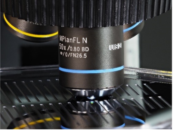
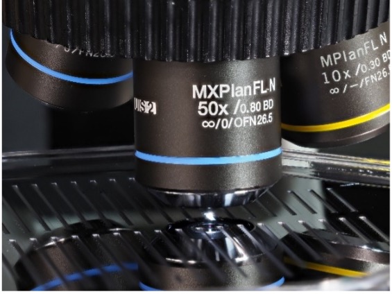
MXPLFLN50X and MXPLFLN50XBD 50X Objectives
The MXPLFLN50X objective is our first 50X objective lens that has achieved a 0.8 numerical aperture and 3 mm working distance simultaneously. Until now, the LMPLFLN100X objective was the only option for both high resolution and long working distance in a single objective. Now, the newly designed MXPLFLN50X objective combines high resolution with a broad working distance. It also provides 4x the viewing field of the LMPLFLN100X objective. This wider field of view helps to shorten inspection times for improved throughput. A brightfield/darkfield version objective type has also been added to the series.
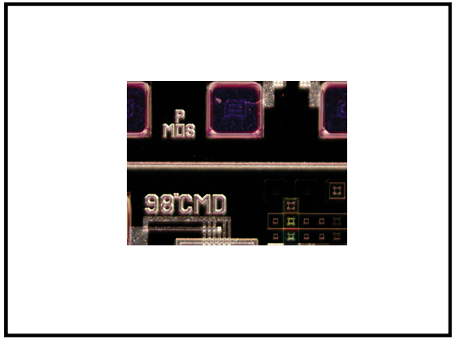 LMPLFLN100X (0.8 NA, 3.4 mm WD) | 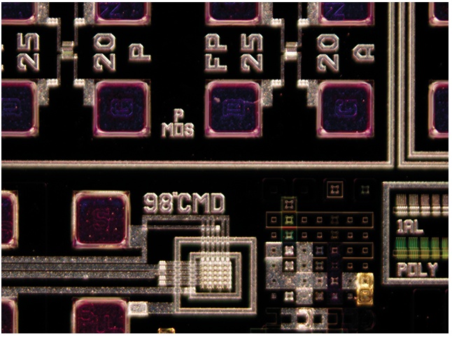 MXPLFLN50X (0.8 NA, 3 mm WD) |
Comparing the field of view. The MXPLFLN50X objective (right, 50X magnification) has a wider field of view than the LMPLFLN100X objective (left, 100X magnification), enabling faster image stitching.
The Advanced Manufacturing Technology Behind the MXPLFLN Objective Series
With a rich history in optical design, Evident is known for producing high-quality objective lenses. After setting a working distance of 3 mm as our goal, we used our design expertise to achieve high-resolution imaging for this working distance.
Achieving high resolution and a long working distance in an objective traditionally would require a large lens diameter and an increased ray height. To resolve this, we developed our new MXPLFLN objective series with a new glass material, which incorporates multiple low-dispersion glass types that are now standard in our high-resolution premium objective lenses. The objectives also feature a special dispersion glass, which is rarely used in reflected light or metallurgical objective lenses. This glass effectively corrects both longitudinal and lateral chromatic aberrations.
Also, by using the ultra-thin lens technology developed for our high-performance X Line™ objective series, we achieved both high resolution and high flatness for enhanced image quality. Our lens manufacturing process also follows strict standards to achieve stable product quality. This includes using wavefront aberration control technology to limit variations in the optical performance of the objective lenses.
Learn More about MXPLFLN Objectives and Other High-Quality Optical Components
To learn more about the benefits of using MXPLFLN objectives for semiconductor inspections and other applications, watch the video below:
We also provide a range of other high-quality optical components that can be combined with your device designs. Head to our OEM resource center to find resources, tools, and FAQs for designing advanced optical instruments.
Related Content
Brochure: MXPLFLN Series for High-Throughput Inspections
Blog: Mix Observation Methods to See More in Your Wafer Defect Inspection
Blog: A Smart Way to Control Contamination for High-Throughput Metrology and Inspection