![]()
Inspecting Printed Wiring Boards
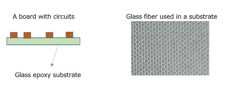
Printed circuit boards with small components mounted to them are used in almost all electronic devices. The area where components are mounted is called a printed wiring board (PWB). The PWB’s base is made of a resin-soaked, glass-fiber-woven fabric. Copper circuits are etched on the substrate. When the etching is complete, small electronic components are ready to be added to the board.
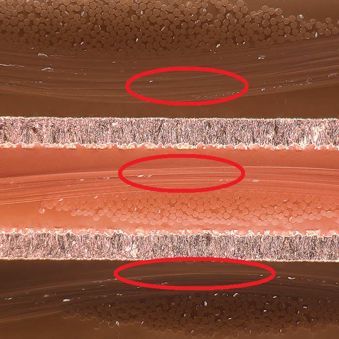
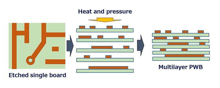
As electronics get smaller, the use of multilayer PWBs has become a necessity. They are fabricated by laminating several boards so that many electronic components can be mounted in a small area. The boards are laminated under pressure while their resin is softened with heat. During this process, the resin can peel and separate from the glass substrate. This kind of flaw is common in the laminated glass fiber or around the edge of a multilayer board.
Resin peeling defects can cause a completed PWB to have lower insulation and heat resistance, making them more susceptible to failure, so inspecting for these defects is critical. Most manufacturers inspect PWBs with an automated system to identify potential problem areas as well as with magnifying lenses. Under the lens, areas of peeling look whiter than the surrounding substrate. If material separation is detected, the area is cut out and examined using a light microscope or digital microscope to determine the cause. However, the reflectivity of the glass substrate makes brightfield observation impossible, so inspectors use polarized light.
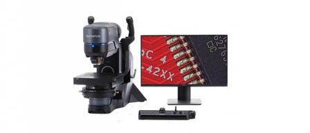
Inspecting PWBs with the DSX1000 Digital Microscope
PWBs are challenging to inspect with a microscope. To determine the cause of a flaw, the board is cross-sectioned and etched. The etching process makes the edges uneven, so it can be hard for a microscope to focus on it properly. If an inspector is examining the etched edge under low magnification, the depth of focus may not be deep enough to provide a clear image. Under high magnification, the image may still be blurry due to poor resolution.
The DSX1000 digital microscope has advanced telecentric optics and high-resolution objectives that offer an excellent depth of focus. These features enable you to observe an etched PWB to investigate the cause of a defect.
Another challenge when inspecting a PWB with a microscope is that the boundary between the glass fiber and resin layers may not be clear. To solve this challenge, the DSX1000 digital microscope has a feature where, by pressing a button, the system will automatically emphasize the sample’s texture, resulting in a clearer image.
*To guarantee XY accuracy, calibration work must be undertaken by an Olympus service technician.
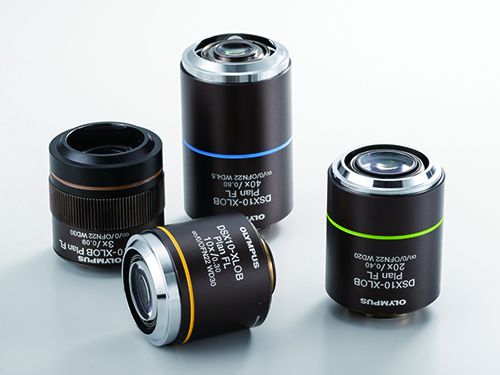
XLOB series objectives
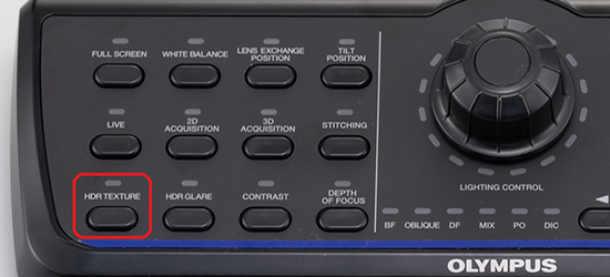
Emphasize texture button
Images
Brightfield image
|
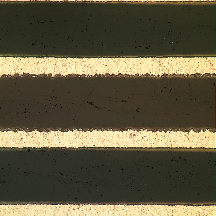
Darkfield image
Darkfield provides a clear image of the layered glass fiber. |