Background
Antenna-coupled nanothermocouples (ACNTCs) for infrared (IR) detection are based on the wave nature of IR radiation. An antenna, its length matched to the incident radiation, receives the electromagnetic waves, and the radiationinduced currents of the antenna heat the hot junction of a nanothermocouple (NTC) (Fig. 1). The heart of these devices is the NTC that converts the heat to electrical signals by the Seebeck effect. Recently, a research group at the University of Notre Dame, including Dr. Gergo P. Szakmany, Prof. Gary H. Bernstein, Prof. Alexei O. Orlov, and Prof. Wolfgang Porod, invented single-metal nanothermocouples that exploit the size-dependent Seebeck coefficient in nanowires. Single-metal NTCs are less complex and less costly to manufacture since they require only one lithography and deposition step. | 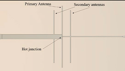 Figure 1. Schematic of an antenna-coupled nanothermocouple for IR detection. The antennas receive the incident radiation and heat the hot junction of the nanothermocouple. |
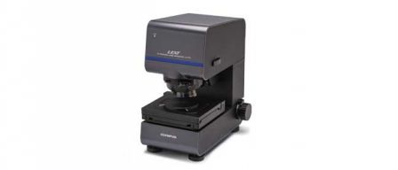
The open-circuit voltage response of an ACNTC is inversely proportional to the heat removal effect of adjacent structures and material, so it is undesirable for the ACNTCs to have direct contact with the substrate. In order to thermally isolate the ACNTCs, the Notre Dame team fabricated suspended ACNTCs over an air-filled cavity, which resulted in an almost 100-fold increase of the device response compared to devices without thermal isolation. Experimental results show that the response of the ACNTC is cavity-depth dependent because, in addition to increasing thermal isolation, the cavity reflects the IR waves back to the antenna causing either constructive or destructive interference. Therefore, the characterization of the physical dimensions of the cavities is critical to understanding device behavior. The group selected the Olympus LEXT™ OLS5000 laser scanning confocal microscope for this purpose. The OLS5000 microscope is an excellent tool for quick, accurate, and nondestructive measurements of cavity depths and profiles. It also provides outstanding resolution for imaging the sub- 100 nm components of the ACNTCs.
Olympus Solution
For some time, the group relied on Notre Dame’s focused ion beam (FIB) instrument to cross-section the cavities and perform a single-profile measurement across the cut line. This process requires the deposition of platinum over the entire substrate in order to create sharp profile edges, and then a lengthy etch step for a depth at least as deep as the cavity. Finally, the cross-section is imaged using the scanning electron microscope capability of the FIB. Because the cost of such a dual-beam system is upwards of $2 million, this process is expensive, as well as timeconsuming and destructive. As an alternative, the group selected the Olympus LEXT™ OLS5000 laser scanning confocal microscope to provide profile information over the entire cavity (Fig. 2) rather than just a single line, as was the case with the FIB. The OLS5000 microscope measures the profile of the cavity in its entire volume, whereas the FIB performs a profile just along the cross-section line. The nondestructive nature of the OLS5000 microscope enables the team to inspect the devices at any step of the fabrication and after electrical and IR testing because no special sample preparation is required that would otherwise destroy the sample. The team also chose the OLS5000 over stylus-based profilometers and an atomic force microscope (AFM) because the OLS5000 microscope can measure steep sidewall profiles and can reach down to the bottom of deep cavities. The stylus tip of the profilometer can collide with the sidewall, and when measuring with the AFM, the depth is limited to a few microns. The stylus and AFM tip can also damage the suspended ACNTCs. In addition, all the alternative methods (FIB, stylus-based profilometer, and AFM) are much slower and, therefore, less cost-effective. While it takes about 1.5 hours to measure the depth of a single cavity with the FIB, it takes less than 3 minutes to obtain more-comprehensive results with the Olympus LEXT OLS5000 laser scanning confocal microscope.
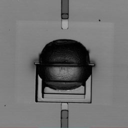 | 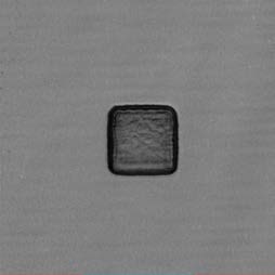 |
Figure 2. (a) A laser-scanning image shows the damaged cavity caused by the FIB. (b) An undamaged cavity. The OLS5000 microscope is nondestructive; cavities can be imaged at any point during the process flow of the device.
Etch depth measurement: At the University of Notre Dame, the ACNTCs are fabricated on a silicon (Si) wafer using electron beam lithography, metal deposition, and lift-off techniques. After the ACNTCs are fabricated, the cavities are formed by xenon difluoride (XeF2) etching of the Si substrate. Pressure and etch time determine the cavity depth and width. The cavity depths ranged between 1 μm and 25 μm (Figs. 3 and 4). At one point, the researchers tried to use an atomic force microscope (AFM) to determine the cavity depth and width, but the AFM was limited to 5 μm-deep cavities and could not reach the bottom of deeper cavities. The OLS5000 microscope measures the depth of the cavity (Fig. 3) accurately, more easily, and much faster than the AFM.

Figure 3. Cavity depth measurement. The OLS5000 microscope quickly provides the depth of a cavity between two points.
Cavity profile measurement: Because of the isotropic nature of XeF2 etching, the profile of the cavities is spherical. Therefore, the cavity not only acts as thermal isolation but also reflects the IR waves back to the antenna, causing either constructive or destructive interferences, depending on the depth of the cavity and the wavelength of the radiation. As a result, the responses of the ACNTCs oscillate with cavity depth. The researchers used numerical simulations to support the experimental results. For accurate simulation, the profile of the cavity had to be precisely determined, because the simple assumption to model the cavity as a sphere was not sufficiently accurate. The OLS5000 microscope made it possible to create a 3D profile of the cavity (Fig. 4) for the simulator using CAD software (Fig. 5). The 3D profile was created either using the 2D line profile (Fig. 4c) and rotational symmetry of the cavity or exporting the 3D image of the cavity to CAD (Figs. 4a and 4b). As a result, the simulation confirmed the assumption that the cavities are creating constructive and deconstructive interferences.
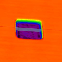 | 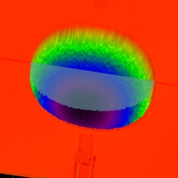 |
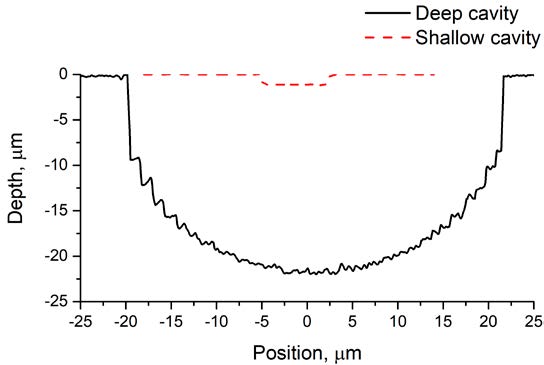
Figure 4. Cavity profile measurements. (a) A 1.07 μm-deep cavity, and (b) a 21.94 μm-deep cavity. (c) The profiles of the two cavities. The OLS5000 microscope proves to be an excellent tool to map shallow and deep cavities.
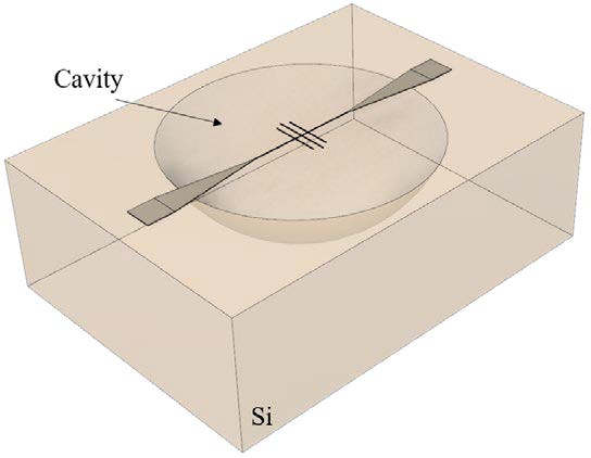
Figure 5. CAD model of the cavity constructed from the cavity profile measurements.
Imaging the ACNTCs: The primary and secondary antennas are a few microns long and are completely suspended over the cavity. As a result, they are susceptible to fabrication errors. The team found that the OLS5000 microscope is able to resolve the sub-100 nm-wide wires of the ACNTCs and provides a quick assessment of device integrity (Figs. 6 and 7) immediately after the fabrication. While currentvoltage (IV) characterization of the devices shows the electrical continuity, it does not provide any information about the geometrical distortions of the antennas (Fig. 8) that could cause a device to underperform. The OLS5000 microscope enables the researcher to select devices for wire bonding and IR testing. The use of scanning electron microscopy is not suitable prior to IR testing because the sample has to be coated with a thin metal layer to avoid charging. Such a process is destructive in that it can electrically short the devices. In addition, improper handling of the sample during SEM scanning could result in ESD damage of the devices. Being able to simultaneously perform 3D profiling of the cavity and evaluate the integrity of the antennas is time efficient and cost effective.
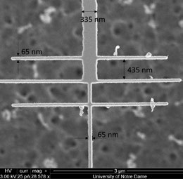 | 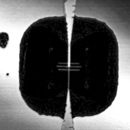 |
Figure 6. a) Scanning electron micrograph of ACNTC. b) LEXT OLS5000 optical micrograph of same device. Excellent image quality and resolution enable a quick inspection of device integrity after fabrication. The center-to-center distance between the horizontal lines is 500 nm and their width is about 65 nm.
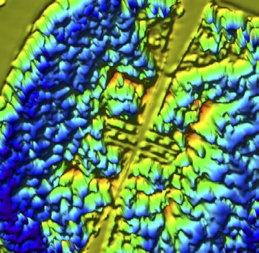
Figure 7. 3D image of the primary and secondary antennas.
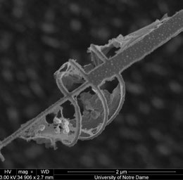 | 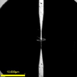 |
Figure 8. Device integrity inspection. (a) SEM of an electrically continuous device and b) the OLS5000 microscope’s image of a similar device; the laser-scanning image shows that the antennas were damaged during the fabrication.
The OLS5000 is equipped with long-WD lenses that provide excellent image quality (Fig. 9). This option enabled the researchers to image the wire-bonded ACNTCs in a chip carrier without removing them.
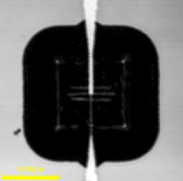
Figure 9. Laser scanning image of a wire-bonded ACNTC taken with the OLS5000 microscope’s long-working-distance lens (LMPLFLN100xLEXT). The long working distance enables imaging of devices in a chip carrier without removing and destroying the sample.
Summary and Conclusions
A group at the University of Notre Dame used the Olympus LEXT™ OLS5000 laser scanning confocal microscope to characterize the geometry of suspended ACNTCs over an air-filled cavity. The OLS5000 microscope provided 3D images and profiles of the cavity. These data were used in numerical simulations to model the devices and support experimental results. The excellent image quality provided invaluable device integrity information after fabrication about the sub-100 nm part of the antenna structure. The physical dimensions of the ACNTC and the cavity were collected accurately, nondestructively, and in a fraction of the time and cost associated with other metrology methods such as FIB, SEM, profilometers, and AFM.
This work was performed in the Notre Dame Integrated Imaging Facility and the Notre Dame Nanofabrication Facility with support from the Notre Dame Center for Nano Science and Technology.
About the Authors
Dr. Gergo P. Szakmany, Dr. Alexei O. Orlov, Dr. Wolfgang Porod, and Dr. Gary H. Bernstein are with the Department of Electrical Engineering University of Notre Dame
The work of G. P. Szakmany was supported by the Notre Dame Joseph F. Trustey Fund for Postdoctoral Scholars.

