Solutions for Electronics (Electronic Device / Semiconductor Industries)
Solutions for Electronics (Electronic Device / Semiconductor Industries)
More information is available on the application notes pages | As electronic devices such as computers, cameras, and smartphones continue to shrink, components like lead frames and connectors are also getting smaller. For example, the average normal distance between electrical connector pins is now only 0.2 mm. In printed circuit boards, very thin plates are coated. Verifying the homogeneity of this coating is a key element of product quality. |
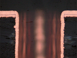
Throwing Power Measurement
Throwing power solution (Cross section of a through hole of PCB) | Use this solution to measure the distribution of copper plating thickness in throughholes or micro-vias through all the steps necessary to make critical measurements of printed circuit boards (PCBs). This includes dimple depth, or the difference in height between the plated copper within a via and around the perimeter of that via. |
Key features
| Typical applications
| Associated functions
|
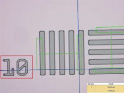
Automatic Critical Dimension Measurement
Automatic measurement solution (Wafer structure) | Use this solution to create edge-detection-based measurements in a live image with pattern recognition. Use the software to create scanners to measure distances (point-to-line, circle-to-circle), circle diameter, circle roundness, and bounding box (width, length, and area). The integrated validation tool provides a pass/fail flag for every measurement. |
Key features
| Typical applications
| Associated functions
|
Other Recommended Solutions
- 3D
- Count and Measure
- Particle Distribution
- Porosity
- Extended Phase Analysis

