Application
Technical innovations in the MEMS (micro-electro-mechanical-systems) market are remarkable; the commercialization of various sensors, ink-jet printer nozzles, medical devices, and other micro-electrical systems is under way in different fields. The shapes, structures, and implementation of MEMS methods are becoming more diverse and complicated. As components become smaller, it is increasingly important to have technology capable of accurately measuring very small areas.
The Olympus solution
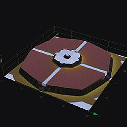
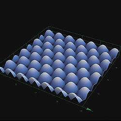
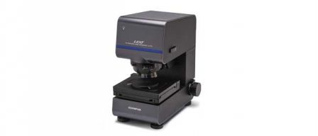
Olympus' LEXT 3D laser scanning confocal microscope enables timely surface profile observations of intricate MEMS structures, surface profile measurements, and provides resolution and accuracy that were previously unavailable. For example, for a sample that is still in a wafer state, the LEXT can capture real-time 3D imaging of the wafer’s cross-section during grinding and determine quality during the etching process; inspectors no longer need to rely on electron microscopes (Figure 1).
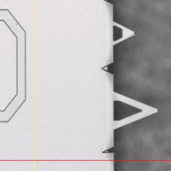
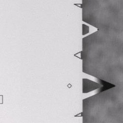
Cantilevered beams are rigid structures anchored only at one end and are important components of many MEMS. If the delicate cantilevered beams become bent, electronic devices may not work properly. The LEXT is equipped for confocal imaging, an observation method for imaging only the area in focus, that can be used to instantly determine if a MEMS-specific cantilever structure is bent. When no bending is present, the microscope obtains an image of the sample entirely in focus (Figure 2, left). However, when bending is present, the deflected area of the sample is not in focus and will appear dark (Figure 2, right). This feature enables inspectors to quickly perform quality assurance on MEMS products.
MEMS 3D shape evaluation | |
Optical MEMS Objective lens Zoom |
Micro lens array Objective lens Zoom |
| Figure 1 | |
Cantilever deflection test using confocal observation | |
Cantilever With deflection
|
Cantilever With deflection
|
| Figure 2 | |
