![]()
Integrated Circuit Manufacturing and Chipping Damage
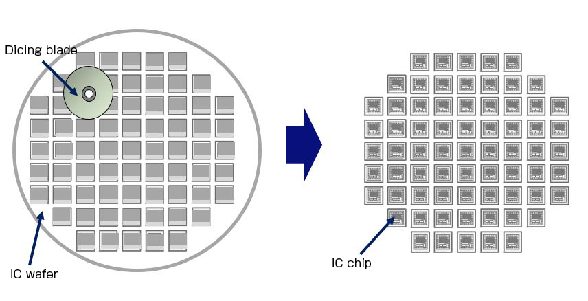
Integrated circuit (IC) manufacturing can be broken down into two processes—forming circuits on bare wafers and packaging. The circuit formation process begins with cylindrical pieces of semiconductor material. The cylinders are sliced into thin, circular pieces called bare wafers. The bare wafers are oxidized, and an intricate, microscopic circuit pattern is added to them through photoresist coatings, pattern printing, etching, impurity diffusion, and planarization. Once the circuits are formed, the circular wafer is cut into small squares with a metal blade or laser during the dicing process. In the packaging process, the diced chips are secured to a metallic plate called a lead frame and packaged with plastic or ceramic components, creating an integrated circuit. The IC chips are eventually mounted to printed circuit boards (PCBs).
During the dicing process, each wafer is cut following predetermined dicing lines. The chips’ edges should be smooth, but due to weak laser power or worn/slow cutting blades, the surfaces can sometimes be too rough (called chipping). Some roughness is always present since the chips are physically cut, but the amount of allowable roughness is carefully controlled. If there’s too much roughness, it can cause the electronic device the chip is part of to fail.
To check the chips’ roughness, most manufacturers use an automated inspection system with low-resolution optics. When potential defects are found, chips are pulled off the manufacturing line, and the amount of roughness is checked with a digital microscope. However, the physical properties of IC chips can be challenging for digital microscopes.
Challenges of Inspecting IC Chips with a Digital Microscope
Low-magnification digital microscope lenses often have low resolution, so shading and flare can occur during observation, obscuring chipping. In addition, chipping inspection usually requires that the distance between the edge of the wafer and the deepest chipping point should be measured. However, most digital microscopes do not provide guaranteed measurement accuracy and repeatability, so the data may not be precise.
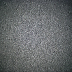 An example of shading | 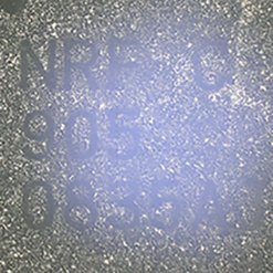 An example of flare |
Advantages of IC Chipping Inspection Using the DSX1000 Digital Microscope
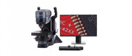
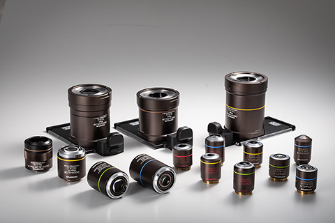
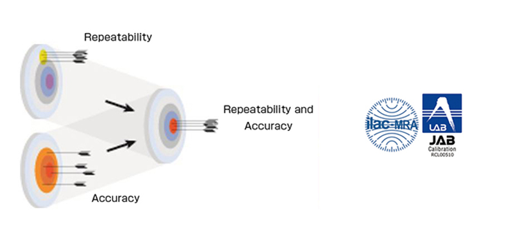
DSX objective lenses offer high resolution at low magnification to reduce shading and flare. This enables inspectors to more easily see chipping during low-magnification observations. The microscope also offers guaranteed accuracy and repeatability*, so inspectors can be confident in their data.
*To guarantee XY accuracy, calibration work must be undertaken by an Olympus service technician.
 An IC chip captured with a conventional microscope | 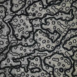 An IC chip image captured using the DSX1000 |
Images
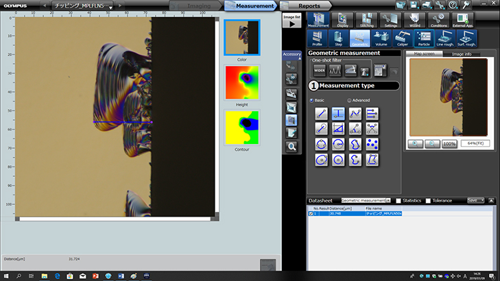 High-precision measurement at 2500X magnification |

