- Home
- 5G Device Measurement and Inspection Solutions
- Fast Failure Analysis
Fast Failure Analysis
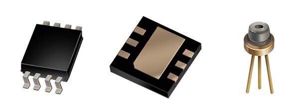
Analyzing Semiconductor Wafers used in High-Frequency DevicesCompound semiconductors can process at high speed and under high voltage, making them ideal for 5G applications. Because they are critical electronic device components, checking them for defects is important.
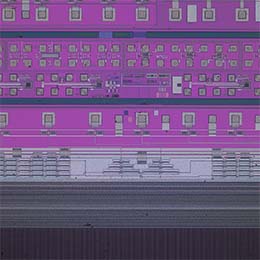
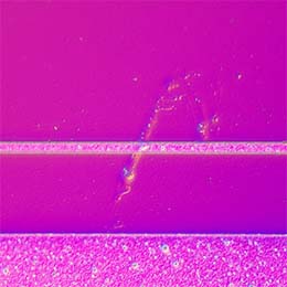
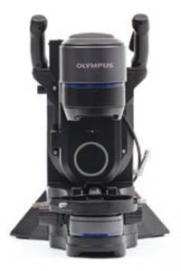
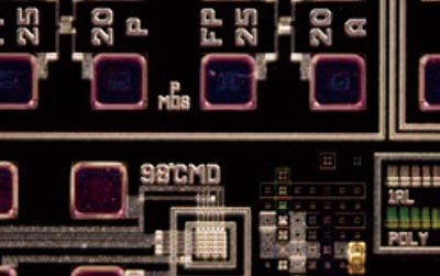
Challenges of Measuring Semiconductor WafersWafers are typically inspected for defects using a metallurgical microscope. One common problem is that it is easy to lose sight of a defect when changing to a higher magnification objective to take a closer look. | Flexible Imaging for Fast Wafer MeasurementThe DSX1000 digital microscope enables you to switch observations—such as differential interference contrast—with the touch of a button. In addition, the microscope’s optical zoom enables seamless macro to micro imaging, so you won’t lose sight of any defects.
Wafer defect DIC observation:
|
Observation of Resist Residues in Semiconductor MaterialsPhotoresist materials play an important role in the etching process for circuit
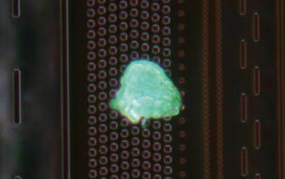
Challenge of Optical Microscope InspectionEven when an optical microscope is used, resist residue can be overlooked. It is important to choose a microscope with the right features for this application. | Easy Detection of Resist ResiduesThe BX53M upright metallurgical microscope supports fluorescence observation, offering an easy solution for the detection of organic resist residues with light-emitting properties. You can distinguish resist residues from other contamination by the differences in their emission characteristics.
|
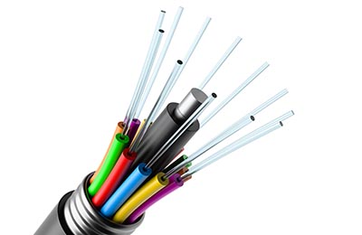
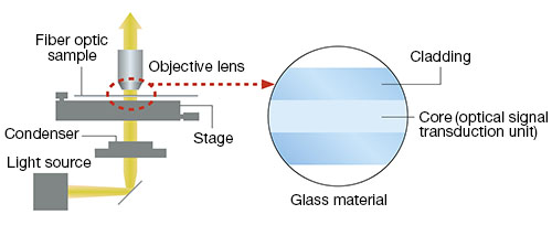
Observing the Molding Condition of Optical Communication WaveguidesManufacturers must validate the molding condition of optical waveguides, which are components used in optical communications. Since an optical waveguide is surrounded by glass, observation using the epi-illumination (reflected light) of a microscope is impossible. Transmission illumination is essential for this application.
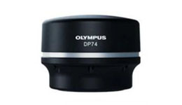
Inspection Challenges Using a Digital or Measuring MicroscopeIt is possible to observe optical waveguides using a transmitted-light measuring microscope or a traditional digital microscope, however, the observation image will typically be blurry or unclear. | Clear Observation of the Molding ConditionWhen combined with the DP74 digital microscope camera, the BX53M upright metallurgical microscope’s high optical performance and differential interference contrast function enable you to clearly observe and capture high-resolution images of the molding condition of an optical waveguide.
|
Need assistance? |
.jpg?rev=FFD6)
.jpg?rev=FFD6)
