Microscope Solutions for
PCB Manufacturing
- Home
- Microscope Solutions for PCB Manufacturing
- Processing the Outer Layer
Processing the Outer Layer
Circuits are formed on both sides of the multilayer substrate using the same process as the inner layer.
Managing the Plating Thickness
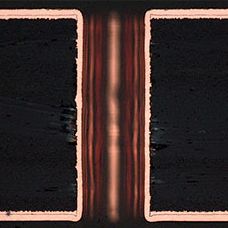
Inspectors must check the thickness of the plated copper on a PCB to make sure that the copper is evenly plated on the board.
Our Solution
Our DSX series digital microscope or BX series metallurgical microscope combined with OLYMPUS Stream™ software enables you to measure the distribution of copper plating thickness in through holes or micro-via with a simple inspection workflow.
BX series metallurgical microscope with OLYMPUS Stream software | 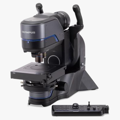 DSX series digital microscope with OLYMPUS Stream software |  Cross-section of a through hole |
Application Notes
Explore related applications:
 |
| ||
 |
| ||
 |
|
BX series metallurgical microscope Request a Quote | DSX series digital microscope Request a Quote |
Measuring the Via Hole Dimensions
The via-hole is used for electric conduction between layers of the substrate pattern. The width and depth of the via-hole must be measured.
Our Solution
Our STM series measuring microscope can measure the dimension of the via hole.
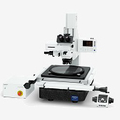 STM series measuring microscope | 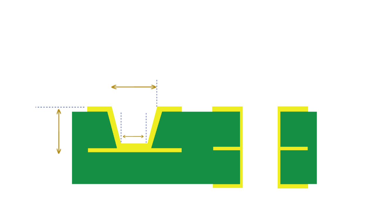 Position to be measured by the STM series microscope |
Application Notes
Explore related applications:
 |
| ||
 |
| ||
 |
|
Checking the Copper Pattern for Defects
Inspectors must check for the presence of defects in copper patterns to help ensure safe, normal power distribution.
Our Solution
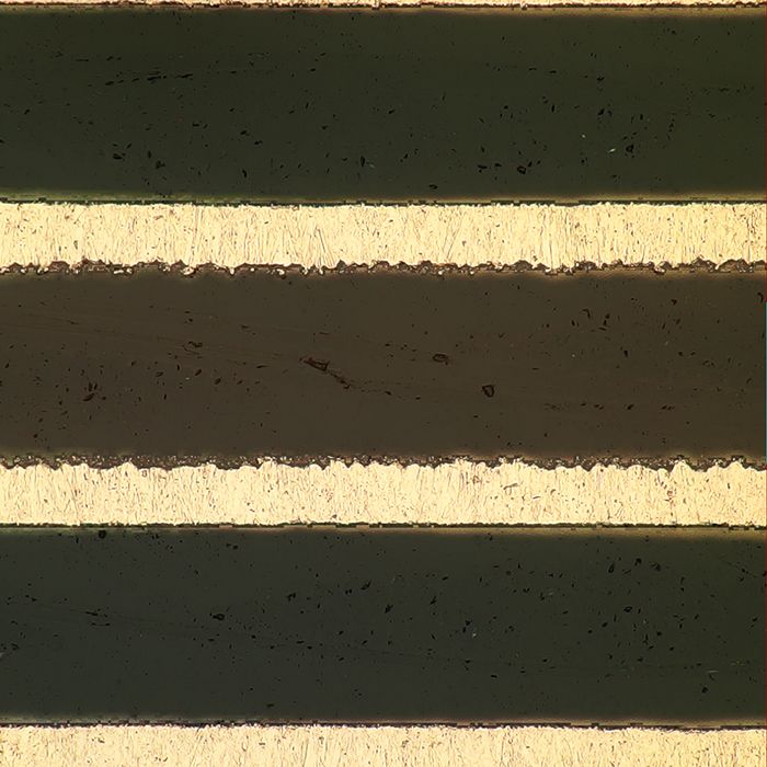
Our DSX series digital microscopes and BX series metallurgical microscopes provide high-magnification observation of defects on copper patterns.
 DSX series digital microscope with OLYMPUS Stream software | BX series metallurgical microscope with OLYMPUS Stream software | 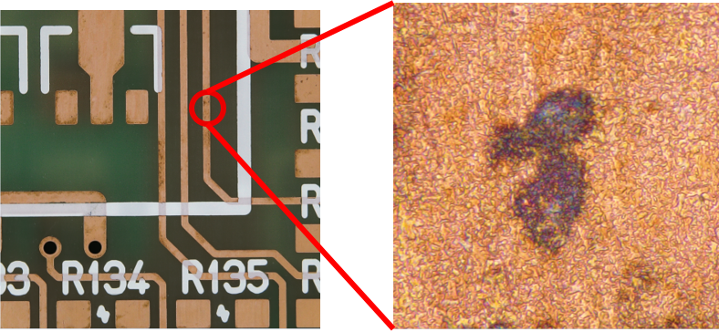 High-magnification image of the copper pattern |
Application Notes
Explore related applications:
 |
| ||
 |
| ||
 |
|
DSX series digital microscope Request a Quote | BX series metallurgical microscope Request a Quote |
Measuring the Copper Pattern
The dimensions of the copper wire can impact electric conduction, so inspectors must measure it to help ensure safe, normal power distribution.
Our Solution
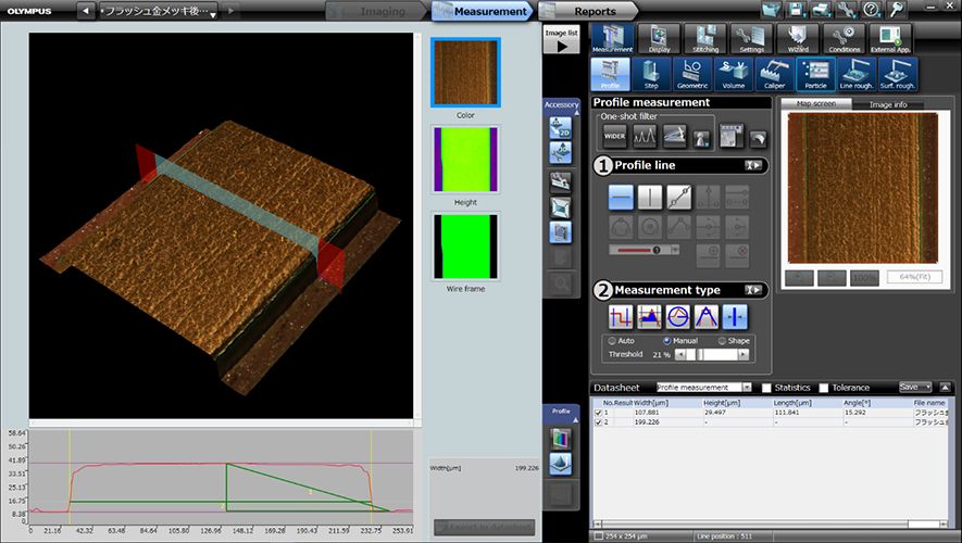
Our DSX1000 digital microscope can provide cross-sectional images of copper patterns in 3D, enabling height and width measurements.
 DSX series digital microscope with OLYMPUS Stream software |  A 3D image of copper pattern |
Application Notes
Explore related applications:
 |
| ||
 |
| ||
 |
|
