Microscope Solutions for
Semiconductor Manufacturing
- Home
- Microscope Solutions for Semiconductor Manufacturing
- Electrical Test
Electrical Test
Check if the wafer runs correctly with an electronics tester called a prober.
Measuring Probe Mark Dimensions
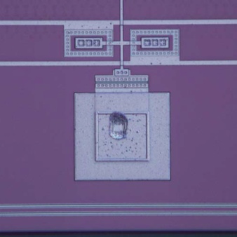
During the electrical test of IC chips, the prober’s testing pin scratches the chips' aluminum pads. If the scratch mark is large, the electrical conductivity conditions on the aluminum pads will decay and affect the wire bonding process. As a result, the dimensions of the scratch marks must be measured.
Our Solution
Our DSX1000 digital microscope can capture 3D images and provide 3D measurements, enabling you to measure the scratch mark’s depth and width.
DSX series digital microscope | Probers |  Prove mark on an aluminum pad |
Application Notes
Explore related applications:
| |||
| |||
 |
|
Not available in your country.
Not available in your country.