Microscope Solutions for
Semiconductor Manufacturing
- Home
- Microscope Solutions for Semiconductor Manufacturing
- Photolithography
Photolithography
Photolithography is the process of imprinting integrated circuit patterns on the wafer. This process is repeated several times to make complex circuit patterns.
Measuring the Resist Thickness in the Photoresist Process
The inspector prints the designed pattern on the silicon wafer using photolithography. Managing the thickness of the resist is critical to correctly print the pattern on the wafer.
Our Solution
With QWP filters, our OLS5000 laser confocal microscope can remove the scattered light effect from the silicon and accurately capture the surface profile. Skip scan mode also helps with fast acquisition.
OLS series laser scanning microscope | Photoresist captured using a MPLAPON100xLEXT objective | Scattered light Remove the affect of scattered light |
Application Notes
Explore related applications:
| |||
|
Checking for Residual Photoresist
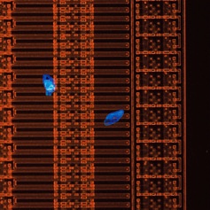
Photoresist must be completely removed from the wafers at the end of the lithography process as its residues cause the electric circuits to malfunction. Residual photoresists are difficult to inspect due to their small size.
Our Solution
The fluorescence observation method on our MX series industrial microscope brightens the residues for easy inspection. Combine the microscope with the optional auto wafer loader for highly efficient inspections.
MX series semiconductor microscope |  Fluorescent observation of residues of photoresist |
Application Notes
Explore related applications:
| |||
|
Checking IC Patterns on a Wafer after Etching
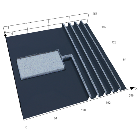
A silicon carbide (SiC) wafer is used as a substrate for a power semiconductor. An inspector checks the pattern dimension on the wafer after etching. As pattern sizes become smaller, accuracy is needed to check them. The pattern (trench) on the SiC wafer must also be measured. The size of the trench on the SiC is around 1 μm.
Our Solution
Our OLS series microscope can measure the fine patterns after etching.
OLS series laser scanning microscope |  Pattern on SiC wafer | Cross section of a SiC wafer |
Application Notes
Explore related applications:
| |||
| |||
|
Detecting Defects on Patterns
Wafers can get defects from degrading manufacturing equipment, inadequate adjustment, human error, and contamination, so it is critical to detect them.
Our Solution
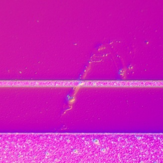
Our MX series and DSX series microscopes can be used to inspect defects. The operator selects a suitable observation method to detect defects with low magnification and confirms the type of defect using high magnification. Our DSX series (with a customized large stage) provides a simple workflow with easy-to-change observation methods.
MX series semiconductor microscope | DSX series digital microscope |  DIC observation with high magnification |
Application Notes
Explore related applications:
| |||
 |
|
MX series semiconductor microscope Request a Quote | DSX series digital microscope Request a Quote |