3.2 方框示意图
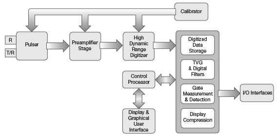
A block diagram of a typical contemporary ultrasonic flaw detector is seen below. In the analog front end, the pulser provides a high voltage impulse to the transducer at a selected pulse repetition frequency, generating the outgoing ultrasonic wave. Echoes returning from the test piece are received by the transducer and converted back into electrical signals, which in turn are fed into the receiver. The echoes are amplified as required and then digitized by a high dynamic rage digitizer module that is capable of handling the wide variation of signal amplitudes commonly seen in ultrasonic NDT. The microprocessor-based control and timing logic synchronizes the pulser and the digitizer, selecting the portion of the wave train that will be further processed and displayed. A calibrator is implemented to calibrate DC offset, gain, phase, and frequency response of the analog front end through the digitizer. This calibration scheme ensures drift free operation, instrument linearity, and unit to unit repeatability that is a major advantage of digital versus analog signal processing in ultrasonic instruments.
Following digitization, the selected echoes from each data acquisition are stored in memory. They are further processed by digital bandpass filters to optimize signal-to-noise. Time varied gain (TVG) is applied if being employed. The processed echoes are then analyzed through gate and time/amplitude measurement software as programmed by the user, compressed as required for display purposes, and displayed on the instrument’s display screen.
