Background
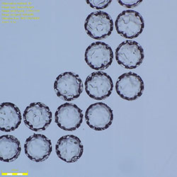
Marking wafers is an essential process in managing semiconductor wafer lots. Normally, silicon wafers are marked with their ID numbers using pulse laser irradiation. Laser irradiation creates dents in the lattice on a silicon wafer surface. These dents form a dot matrix sequence of characters and codes. In recent years, silicon wafers have continued to increase in density while at the same time becoming thinner. This has created a need to further reduce the size as well as to increase the accuracy of the laser marking technology.
Olympus solution
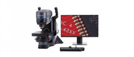
The Olympus DSX digital microscope is equipped with an EFI feature that enables the user to take multiple photos by changing the focus at high speed. This EFI feature is designed to produce clear images by maintaining focus across the entire visual field. This technology makes it easy to capture tack-sharp images of all parts of a silicon wafer. From the wafer surface to the bottom of a laser mark the entire visual field is in focus. The DSX also comes standard with a wide range of measuring features to allow users to accurately measure the diameter of a laser mark, the length of a mark sequence, as well as the depth of a dot.
Features of the product
- High-definition, high-resolution image inspection
- EFI feature designed to maintain focus across the entire visual field
- Software package contains a wide range of measuring features
- Diverse image-processing techniques
- Differential interference contrast
- Guidance features that allow all users to obtain high-quality results
Image

Inspection of Laser Marks on Bare Semiconductor Wafer
Objective Lens 20x , Zoom 1.5x

