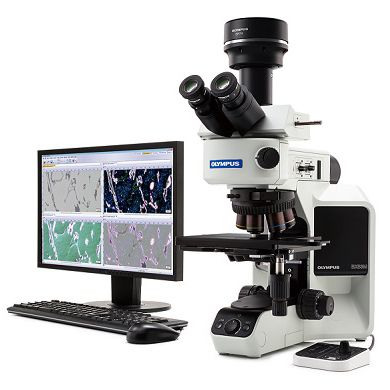
Microscope Solutions for
Semiconductor Manufacturing
Wire Bonding
An IC chip connects to external devices with wire bonding. Wire bonding is a method to weld between an IC chip and the lead frames. A wire is attached to a lead frame and an IC chip's aluminum pad using a combination of downward pressure, ultrasonic energy, and heat to make a weld.
Analyzing the Surface Conditions of Lead Frames
An IC chip and the inner leads of lead frames are connected by bonding wires. Uneven surfaces on the leads can cause faulty adhesive wire bonding, so it is important to measure the leads’ surface roughness. Another challenge is that as IC packages downsize, the leads became thinner.
Our Solution
Our OLS series microscope can image ultra-fine leads for roughness measurement. Roughness of the lead frame is managed by an R ratio, and the OLS series has the necessary parameter.
OLS series laser scanning microscope | Microscope image | 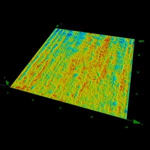 Surface roughness |
Application Notes
Explore related applications:
| |||
| |||
|
Checking the Position of Mashed Balls
Mashed balls (the ball-shaped ends of bonding wires) must be placed in certain positions on aluminum pads to transfer electric signal. If the mashed balls are placed outside of the pad, the bonding machine settings must be adjusted. As a result, inspectors must check the mashed ball positions.
Our Solution
Our STM series measuring microscope with high magnification can measure the mashed ball positions with high magnification.
STM series measuring microscope | 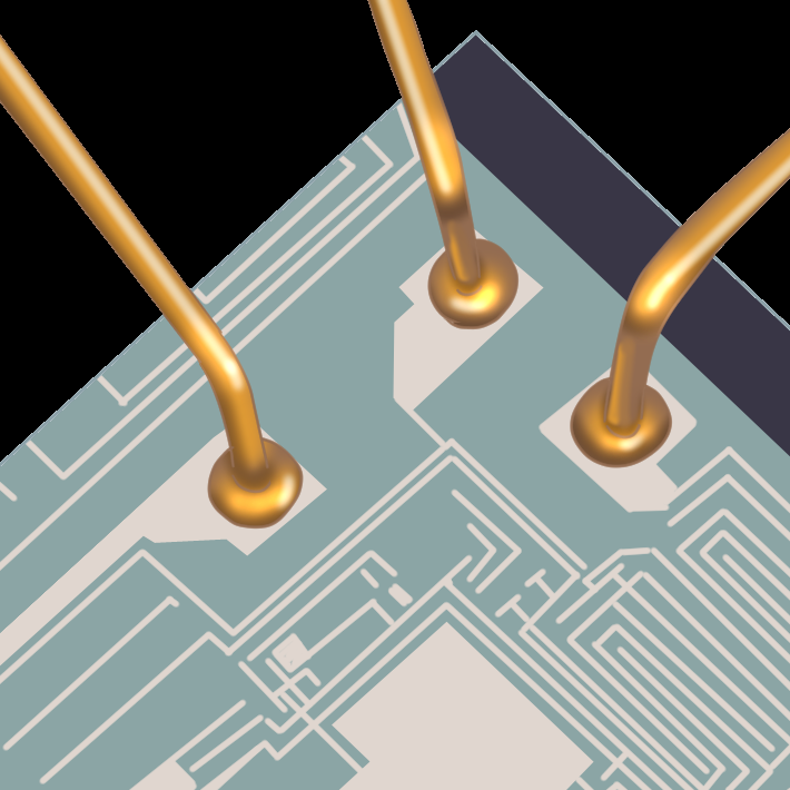 Mashed ball | A ball placed outside of a pad |
Application Notes
Explore related applications:
| |||
| |||
 |
|
Measuring the Height of Wire Loops
Since short circuits occur if a bonded wire touches an IC chip or package, the height of wire loop must be controlled. It is difficult to perform the height measurement of wire loops at an affordable price as the wire is very thin and the wire loop is very small. The wires and IC chip also must be treated using a noncontact method.
Our Solution
Our STM series measuring microscope with a long working distance, high-magnification lens (>50X) can accurately measure the loop height. Optional items such as the autofocus or focus navigator function can improve the measurement efficiency and accuracy.
STM series measuring microscope | Loop height of bonding wire |
Application Notes
Explore related applications:
| |||
| |||
 |
|
Checking for Defects on Bonding Wires
The bonding wire width can be as thin as 15–30 μm. Even a small failure in the wire bonding will impact the electric transfer of signals. These small failures are very difficult to detect with visual inspection.
Our Solution
Our DSX1000 digital microscope can detect small defects such as cracks and scratches on bonding wires.
DSX series digital microscope | 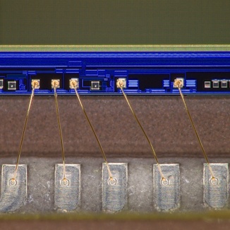 Bonding wire (75X) | 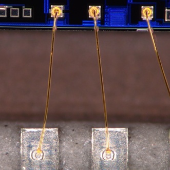 Bonding wire (150X) |
Application Notes
Explore related applications:
| |||
| |||
|
Checking for Splashes from an Aluminum Pad
Splashes from an aluminum pad can occur during ultrasonic welding. If a splash touches the next pad or a connection area between a ball and pad, it will cause a short circuit. In this case, changing the ultrasonic setup is required to reduce splashes.
A scanning electron microscope (SEM) is typically used for this inspection, but this method can be time-consuming. it is also difficult to detect splashes using an interferometer.
Our Solution
Our OLS5000 laser confocal microscope can detect splashes from an aluminum pad.
OLS series laser scanning microscope | 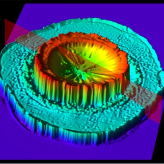 |
Application Notes
Explore related applications:
| |||
| |||
 |
|
Checking Void and Corrosion in a Welding Area
Voids and corrosion in a welding area impact electric signal transmission, so checking for voids or corrosion is required. If voids or corrosion are found, then the welding strength must be adjusted.
A scanning electron microscope (SEM) is typically used for this inspection, but this method can be time-consuming.
Our Solution
Our OLS5000 laser confocal microscope can capture an image at 9,000X magnification, enabling you to quickly observe cross sections of a welding area.
OLS series laser scanning microscope |  Voids in a welding area |
Application Notes
Explore related applications:
| |||
| |||
|
Infrared (IR) Inspection
A flip chip is a type of integrated circuit (IC) chip that has electrode terminals on its back surface. Its design helps to reduce the mounting space on a printed circuit board. Improper bonding and damaged IC patterns on the flip chip can cause malfunctions, yet it is difficult to inspect them since they are inaccessible after packaging.
Our Solution
The IR imaging capabilities of our BX and MX industrial microscope series enable you to perform nondestructive internal observation of a flip chip after packaging due to the transmission properties of silicon. This inspection method is also used for MEMS wafers.
BX series metallurgical microscope with IR unit | MX series semiconductor microscope with IR unit | Flip-chip |
Application Notes
Explore related applications:
| |||
| |||
|
BX series metallurgical microscope | MX series semiconductor microscope |
