处理外层
使用与制作内层相同的工艺在多层基板的两面形成电路。
管理镀层厚度
检测人员必须检查印制电路板(PCB)上铜镀层的厚度,以确保铜镀层均匀地平铺在电路板上。
我们的解决方案
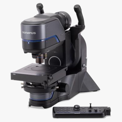
我们的DSX系列数码显微镜或BX系列金相显微镜与OLYMPUS Stream软件配套使用,可使您通过简单的检测工作流程来测量通孔或微型导通孔中铜镀层厚度的分布情况。
带有OLYMPUS Stream软件的BX系列金相显微镜 | 带有OLYMPUS Stream软件的DSX系列数码显微镜 |  通孔的横截面 |
应用注释
探究相关应用:
 | |
使用图像分析软件测量分散能力或PCB铜镀层厚度的均匀性
| 阅读更多内容 |
|
 | |
清晰的图像是成功完成质量控制的关键:检测印制电路板玻璃环氧基板中玻璃纤维的剥落情况
| 阅读更多内容 |
|
 | |
测量导通孔尺寸
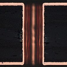
导通孔起到在各层基板图面之间的电传导作用。必须测量导通孔的宽度和深度。
我们的解决方案
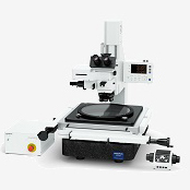
我们的STM系列测量显微镜可以测量导通孔的尺寸。
STM系列测量显微镜 | 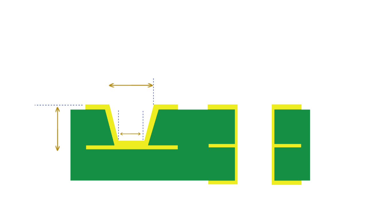 可由STM系列显微镜测量的位置 | |
应用注释
探究相关应用:
| |
 | |
| |
使用图像分析软件测量分散能力或PCB铜镀层厚度的均匀性
| 阅读更多内容 |
|
检查铜制图面是否有缺陷
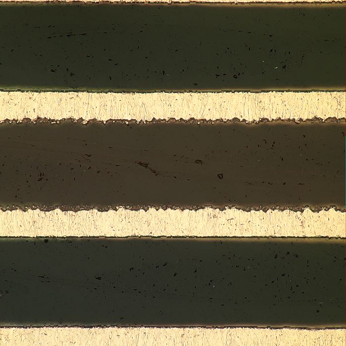
检测人员必须检查铜制图面中是否存在缺陷,以确保实现安全、正常的配电。
我们的解决方案
我们的DSX系列数码显微镜和BX系列金相显微镜可对铜制图面上的缺陷进行高倍放大观察。
带有OLYMPUS Stream软件的DSX系列数码显微镜 | 带有OLYMPUS Stream软件的BX系列金相显微镜 | 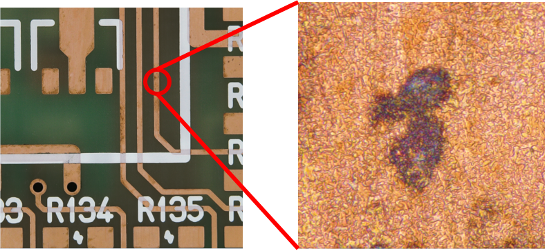 铜制图面的高倍率图像 |
应用注释
探究相关应用:
 | |
 | |
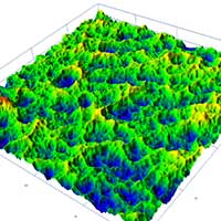 | |
使用奥林巴斯OLS5000激光共聚焦显微镜测量印制电路板的表面粗糙度
| 阅读更多内容 |
|
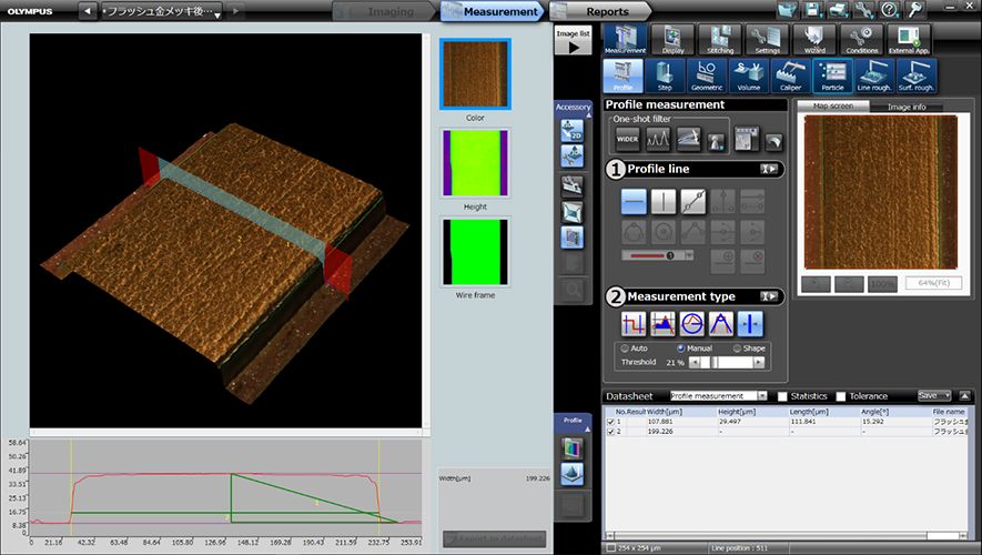
测量铜制图面
铜线的尺寸会影响导电效果,因此检测人员必须对其进行测量,以确保实现安全、正常的配电。
我们的解决方案
我们的DSX1000数码显微镜可以提供铜制图面横截面的三维图像,有助于进行高度和宽度测量。
带有OLYMPUS Stream软件的DSX系列数码显微镜 | 铜制图面的三维图像 | |
应用注释
探究相关应用:
| |
| |
使用奥林巴斯OLS5000激光共聚焦显微镜测量印制电路板的表面粗糙度
| 阅读更多内容 |
|
| |
使用图像分析软件测量分散能力或PCB铜镀层厚度的均匀性
| 阅读更多内容 |
|
Not available in your country.
Not available in your country.
Sorry, this page is not available in your country